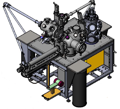
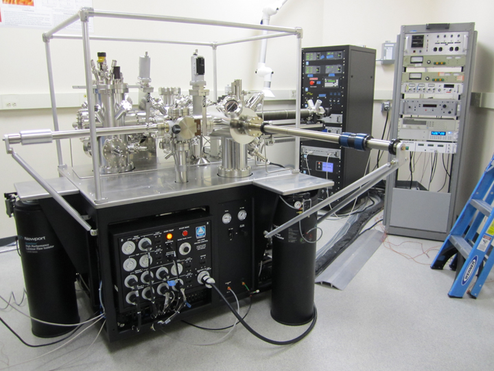
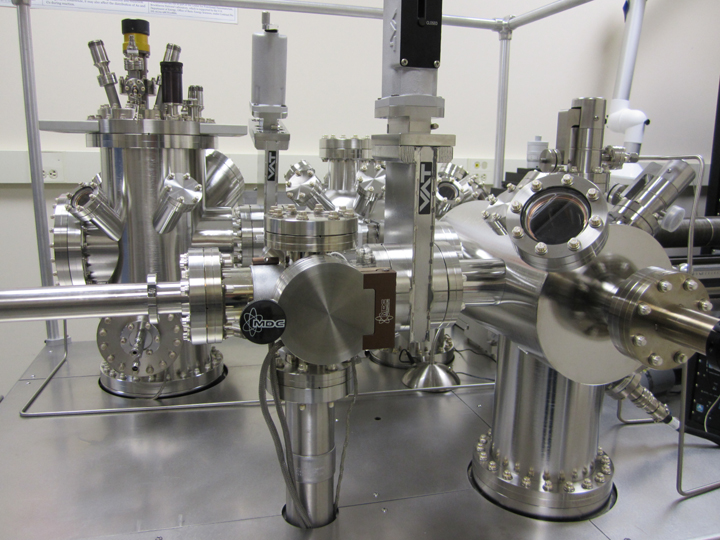
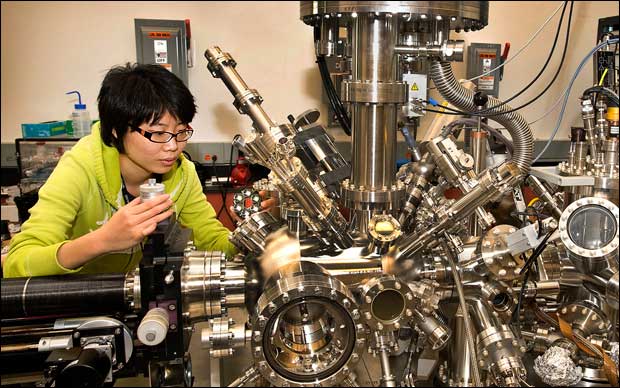
Our lab is equipped with a STM/AFM/AES/LEED system for studying surface and interface reactions.


The system consists of four interconnected UHV chambers: a load lock for fast sample transfer, a sample preparation chamber, a surface analysis chamber, and a scanning tunneling microscopy chamber (variable temperature STM). The system features scanning tunneling microscopy, atomic force microscopy, Auger electron spectroscopy, low-energy electron diffraction, Argon ion sputter gun, and electron beam evaporator |
In addition, the Analytical and Diagnostics Laboratory (ADL) at Binghamton University houses extensive facilities for materials nanofabrication and nanocharacterization. These include an electron microscopy suite, a laser microscopy lab, X-Ray imagers, a general microscopy suite, a surface analysis suite, a microfabrication laboratory, and a thermal analysis suite. We has full access to these instruments. Click here for more information on the ADL.
The Center for Functional Nanomaterials (CFN) at Brookhaven National Laboratory is one of four DOE user facilities. Along with a variety of other unique and state-of-the-art instrumentation, it houses a FEI Tatan environmental TEM with an aberration corrector, specializing on high resolution in situ microscopy of chemical reaction processes, and a suite of surface science tools including in-situ XPS, ambient-pressure XPS, high-pressure reactor-STM, and low-energy electron microscopy (LEEM). Postdocs and graduate students in our group have been frequently using these instruments for their research projects. Click here for more information on CFN.
Last Updated: 5/10/12